Fact-checked by the ZeroinDaily editorial team
Quick Answer
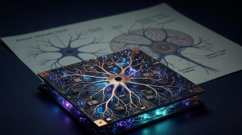
Neuromorphic chips are processors modeled on the human brain’s neural architecture, using spiking neural networks to process data with radical energy efficiency. Intel’s Hala Point system, built on its Loihi 2 chip, contains 1.15 billion neurons and runs up to 100x more efficiently than conventional GPUs on AI workloads.
Updated July 2026
These processors are designed to mimic the way biological neurons communicate, through electrical spikes rather than continuous computation. This event-driven design enables them to operate with extreme energy efficiency, especially in environments where real-time processing and low power are critical. The neuromorphic computing market was valued at $7.24 billion in 2025, according to Polaris Market Research’s 2026 analysis, and patent filings in the space surged 401% in 2025 alone, per PatSnap data.
That growth is being driven by a hard physics ceiling: traditional von Neumann processors are running out of room to scale, while AI inference demands keep rising. Neuromorphic architecture offers a credible path forward, one that is already moving from the lab into products.
Key Takeaways
- Neuromorphic chips use spiking neural networks that fire only on meaningful input, slashing idle power draw to near zero. Intel’s Loihi 2 demonstrates up to 1,000x better energy efficiency than CPU inference on sparse AI workloads.
- The global neuromorphic computing market hit $7.24 billion in 2025, with patent activity jumping 401% the same year. Source: Polaris Market Research, PatSnap.
- IBM’s TrueNorth chip integrates 1 million neurons and 256 million synapses while consuming just 70 milliwatts. Source: Human Unsupervised, citing original IBM research.
- DARPA allocated $75 million to neuromorphic chip R&D in fiscal year 2025 through its Electronics Resurgence Initiative. Source: Market Intelo.
- Neuromorphic chips are not GPU replacements. They are complements, optimized for sparse edge inference rather than dense training. The tradeoff: SNNs are harder to program and lack mature tooling like PyTorch or TensorFlow.
- The European Human Brain Project has connected over 3,000 researchers to neuromorphic platforms, and a $4 million NSF grant in 2025 established The Neuromorphic Commons (THOR) hub at UTSA. Source: UTSA.
How Do Neuromorphic Chips Actually Work?
Neuromorphic chips process information using spiking neural networks (SNNs), circuits that fire electrical pulses only when a threshold is crossed, just like biological neurons. This event-driven model means the chip does nothing when there is no meaningful input, slashing idle power draw to near zero.
Conventional processors move data back and forth between a central processor and separate memory, a bottleneck called the von Neumann bottleneck. Neuromorphic chips integrate memory and computation at the same physical location, in structures called synapses. This co-location eliminates the energy cost of constant data shuttling.
Spiking Neural Networks vs. Standard Neural Networks
Standard deep learning runs continuous floating-point math across all nodes simultaneously. SNNs, by contrast, activate only the nodes that receive a spike above threshold. The result is sparse computation: only a small fraction of the network is active at any moment, which is why Intel Research reports Loihi 2 achieves up to 1,000x better energy efficiency than CPU-based inference on certain sparse tasks.
Key Takeaway: Neuromorphic chips use spiking neural networks that activate only on meaningful input, eliminating the von Neumann bottleneck. Intel’s Loihi 2 demonstrates up to 1,000x better energy efficiency than CPU inference on sparse AI workloads.
Who Are the Key Players in Neuromorphic Chips Explained Across Industry?
Intel, IBM, BrainScaleS, and a growing cohort of startups are the primary forces shaping this field. Each organization takes a meaningfully different architectural approach, which makes direct comparisons instructive.
Intel’s Loihi 2, released in 2021, supports up to 1 million neurons per chip and has been scaled into the Hala Point research system at Sandia National Laboratories. According to SNS Insider, Hala Point simulates 1.15 billion artificial neurons. IBM’s TrueNorth chip, developed in collaboration with DARPA, packs 4,096 neurosynaptic cores and 256 million programmable synapses into a design that draws just 70 milliwatts at full operation, as documented by Human Unsupervised citing the original IBM research.
On the startup side, BrainChip Holdings has commercialized its Akida chip for edge inference, while SpiNNaker, developed at the University of Manchester, focuses on large-scale neural simulation for neuroscience research. The broader AI hardware landscape is also relevant: if you follow how AI is reshaping business tools, our coverage of AI tools saving small businesses time in 2026 shows the downstream commercial pressure driving this chip race.
| Chip / System | Developer | Neuron Count | Power Draw | Primary Use Case |
|---|---|---|---|---|
| Loihi 2 / Hala Point | Intel | 1.15 billion (system) | ~2.6 kW (system) | Research, edge AI |
| TrueNorth | IBM | 1 million | 70 mW | Pattern recognition |
| Akida | BrainChip | Up to 1.2 million | Under 1 W | Edge IoT inference |
| SpiNNaker 2 | Univ. of Manchester / TU Dresden | 10 million (per board) | ~5 W (per board) | Neural simulation |
| BrainScaleS-2 | Heidelberg University / HBP | 512 per chip | ~1 W | Neuroscience research |
Key Takeaway: The neuromorphic chip landscape spans Intel, IBM, and BrainChip, each targeting different scales and use cases. IBM’s TrueNorth draws just 70 milliwatts at full operation, a benchmark that illustrates the radical efficiency gains possible over conventional AI accelerators. Full specs are documented via Human Unsupervised’s analysis of IBM’s foundational research.
What Are the Real-World Applications of Neuromorphic Computing?
Neuromorphic chips are most compelling in scenarios that demand low-latency, low-power AI at the edge, places where cloud round-trips are too slow or too costly. Three domains stand out: autonomous systems, healthcare wearables, and smart sensors.
In robotics, neuromorphic processors handle sensory-motor integration faster than traditional chips because they respond to events rather than polling data at fixed clock cycles. Intel’s collaboration with researchers at Johns Hopkins University demonstrated a prosthetic hand controlled by Loihi that responded to tactile input in under 1 millisecond, a response time impossible with conventional inference pipelines.
Here is a concrete scenario. Suppose you are designing an autonomous inspection drone for offshore oil platforms. The drone needs to run real-time obstacle avoidance on a tight power budget. A neuromorphic chip like IBM’s TrueNorth draws just 70 mW. A typical edge GPU module for the same task (something like an NVIDIA Jetson) draws around 15W. Over a 30-minute flight, the GPU consumes 7.5 watt-hours. The neuromorphic chip consumes 0.035 watt-hours. That 214x difference means the drone’s battery can dedicate far more energy to motors and payload, extending flight time or reducing battery weight. For a fleet of 20 drones flying two missions per day, the annual energy cost difference at $0.10/kWh is negligible, but the operational advantage of longer flight endurance is substantial.
Edge AI and IoT Deployments
BrainChip’s Akida chip has been deployed in automotive driver-monitoring systems and industrial anomaly detection. Because it processes only changes in sensor data rather than continuous streams, it fits within the tight power budgets of battery-operated IoT devices. This mirrors the broader shift toward on-device AI described in our article on digital banking trends changing money management, where edge processing is also transforming financial security hardware.
Neuromorphic computing represents a fundamental rethinking of what a processor is. The goal is not a faster von Neumann machine. It is a processor that computes the way nature computes: sparsely, locally, and with extraordinary efficiency. This is the vision driving Intel Labs’ neuromorphic program, which has moved from silicon prototypes to multi-institutional research deployments over the past five years.
Key Takeaway: Neuromorphic chips excel at edge AI tasks, robotics, wearables, and IoT sensors, where latency and power budgets are critical. Intel and Johns Hopkins demonstrated prosthetic hand response times under 1 millisecond using Intel’s Loihi platform, a threshold conventional processors cannot match.
How Do Neuromorphic Chips Compare to GPUs and TPUs?
Neuromorphic chips explained in context of GPUs and TPUs reveal a clear tradeoff: raw throughput versus energy efficiency at the edge. GPUs dominate training workloads; neuromorphic chips target inference and real-time sensing.
A high-end NVIDIA H100 GPU delivers massive parallel throughput for training large language models but draws 700 watts at peak. A neuromorphic chip running a comparable inference task draws milliwatts. The difference is not marginal, it is structural. GPUs are optimized for dense matrix multiplication. Neuromorphic chips are optimized for sparse, event-driven computation, which matches the actual structure of sensory data in the real world.
Google’s TPUs sit between the two: purpose-built for tensor operations with better efficiency than GPUs, but still relying on synchronous, dense computation. On sparse pattern recognition tasks, neuromorphic systems deliver dramatically lower energy per inference compared to GPU baselines, as documented in a 2024 benchmark study published in Nature. The tradeoff is programmability. SNNs are harder to train and less mature in tooling than GPU-based deep learning frameworks like PyTorch or TensorFlow.
To put the efficiency gap into concrete terms, consider a neuroscience lab running a billion-neuron simulation around the clock. Intel’s Hala Point system draws 2.6 kW at full load. Based on Intel’s claim of up to 100x better efficiency than conventional GPUs on these workloads, a GPU cluster delivering equivalent throughput would pull roughly 260 kW. Over a year (8,760 hours), Hala Point consumes about 22,776 kWh. At an industrial electricity rate of $0.10 per kWh, that is $2,277.60 annually. The GPU cluster, at 260 kW, would consume 2,277,600 kWh, costing $227,760 per year. That is a $225,482 difference in electricity alone for a single research installation. The savings multiply quickly when you consider cooling, facility power, and the hardware itself.
Key Takeaway: Neuromorphic chips are not GPU replacements, they are complements, optimized for sparse edge inference rather than dense training. A 2024 Nature benchmark confirmed significant energy-per-inference advantages on sparse workloads versus GPU baselines, at the cost of more complex programming.
What Challenges and Milestones Define the Future of Neuromorphic Computing?
The primary barriers to mainstream adoption are software maturity, standardization, and training complexity. Neuromorphic chips explained at a hardware level are impressive; the software ecosystem has not kept pace.
Training SNNs remains significantly harder than training standard deep neural networks. Backpropagation, the dominant training algorithm, does not directly apply to spiking networks because spikes are not differentiable. Researchers are developing surrogate gradient methods and spike-timing-dependent plasticity rules, but these lack the mature tooling of PyTorch or TensorFlow. Intel’s Lava framework and IBM’s open neuromorphic toolkit are steps toward standardization, but widespread developer adoption remains years away.
Regulation and standardization bodies such as IEEE and the European Human Brain Project (HBP) are actively working on benchmarks and interoperability standards. The HBP’s neuromorphic platform, which includes both SpiNNaker and BrainScaleS systems, has served over 3,000 researchers across Europe. In the United States, UTSA received a $4 million NSF grant in 2025 to establish The Neuromorphic Commons (THOR) Project, a national hub for neuromorphic research. Defense investment is also accelerating: DARPA allocated $75 million to neuromorphic chip R&D in fiscal year 2025 through the Electronics Resurgence Initiative.
For context on how adjacent hardware and software trends are reshaping investment decisions, see our guide to AI-powered investment platforms in 2026, neuromorphic efficiency gains will eventually flow into these systems too. The long-term trajectory also connects to how blockchain and distributed compute are changing financial infrastructure, as neuromorphic edge nodes could underpin next-generation secure transaction processing.
Key Takeaway: Neuromorphic computing’s main bottleneck is software, not silicon. The European Human Brain Project has already connected 3,000+ researchers to neuromorphic platforms, and a $4 million NSF grant to UTSA in 2025 established a national neuromorphic commons. DARPA added $75 million in FY2025 funding, signaling that both civilian and defense sectors see this as a strategic priority.
Related reading: Everything You Need to Know About Password Managers: Bitwarden vs 1Password in.
Frequently Asked Questions
What is a neuromorphic chip in simple terms?
A neuromorphic chip is a processor designed to work like a human brain, using artificial neurons that fire electrical spikes only when needed. Unlike standard chips that run continuous calculations, neuromorphic chips activate only when there is meaningful input, making them extremely energy-efficient for AI tasks.
Are neuromorphic chips better than GPUs?
Neuromorphic chips are not universally better. They excel at specific tasks. For sparse, real-time inference at the edge (robotics, wearables, sensors), they use up to 100x less energy than GPUs. For training large AI models, GPUs remain the dominant choice due to mature tooling and raw parallel throughput.
Which companies make neuromorphic chips?
Intel (Loihi 2), IBM (TrueNorth), and BrainChip (Akida) are the leading commercial developers. University research programs at Manchester (SpiNNaker) and Heidelberg (BrainScaleS) produce systems used primarily in neuroscience. DARPA has funded multiple neuromorphic research programs since the early 2010s.
What is neuromorphic computing used for today?
Current applications include autonomous robotics, prosthetic limb control, industrial anomaly detection, edge IoT sensors, and brain-computer interface research. BrainChip’s Akida chip is deployed in commercial automotive and security camera products.
How is a spiking neural network different from a standard neural network?
Standard neural networks use continuous floating-point values passed across all nodes simultaneously. Spiking neural networks transmit discrete spikes only when a neuron’s activation crosses a threshold, resulting in sparse and asynchronous computation. This event-driven model is why SNNs consume far less energy during inference.
When will neuromorphic chips be in consumer products?
Limited commercial deployment has already begun. BrainChip’s Akida is in automotive driver-monitoring systems available since 2024. Broader consumer integration (smartphones, wearables) is likely in the 2026–2028 timeframe as software tooling matures and production costs fall with scale.
How big is the neuromorphic computing market?
The neuromorphic computing market was valued at $7.24 billion in 2025, according to Polaris Market Research. Patent filings in the field surged 401% that same year, per PatSnap, indicating intense R&D activity across industry and academia.
What is Intel’s Hala Point system?
Hala Point is Intel’s largest neuromorphic research system, built by scaling up Loihi 2 chips. It simulates 1.15 billion artificial neurons, as reported by SNS Insider. The system is deployed at Sandia National Laboratories for large-scale edge AI and computational neuroscience research.
How much power does IBM’s TrueNorth chip use?
IBM’s TrueNorth chip consumes just 70 milliwatts at full operation while integrating 1 million neurons and 256 million synapses, according to Human Unsupervised citing the original IBM research. That is roughly the power draw of a small LED light.
What government funding supports neuromorphic research?
DARPA allocated $75 million to neuromorphic chip R&D in fiscal year 2025 through its Electronics Resurgence Initiative, per Market Intelo. The NSF awarded $4 million to UTSA in 2025 to establish The Neuromorphic Commons (THOR) Project, a national research hub, as announced by UTSA.
Sources
- Intel Labs, Neuromorphic Computing Research
- IBM / Merolla et al., TrueNorth: A Million Spiking-Neuron Integrated Circuit (Science, 2014)
- Nature, Neuromorphic vs. GPU Efficiency Benchmark Study (2024)
- Polaris Market Research, Neuromorphic Computing Market Size and Forecast (2026)
- PatSnap, Neuromorphic Computing Chip Patents Surge 401% in 2025
- SNS Insider, Neuromorphic Chip Market Report
- Human Unsupervised, Neuromorphic Computing Landscape (citing original IBM TrueNorth research)
- University of Texas at San Antonio, NSF Grant Establishes THOR Neuromorphic Commons (2025)
- European Human Brain Project, Neuromorphic Computing Platform