Fact-checked by the ZeroinDaily editorial team
Quick Answer
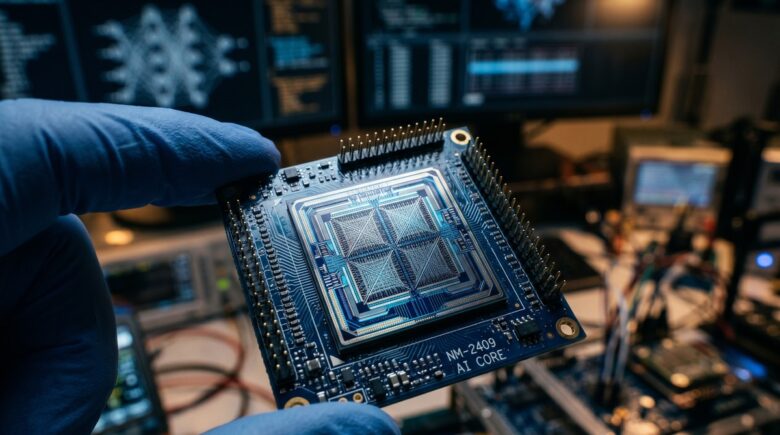
Neuromorphic chips are processors that mimic the structure of the human brain, using spiking neural networks instead of traditional transistor logic. Intel’s Hala Point system contains 1.15 billion artificial neurons, consuming up to 100x less energy than conventional AI accelerators for equivalent inference tasks.
These are semiconductors engineered to replicate how biological neurons fire and communicate, enabling machines to process sensory data with dramatically lower power draw. According to Intel’s neuromorphic computing research division, its Loihi 2 chip processes certain pattern-recognition workloads while consuming fewer than 1 milliwatt, a fraction of what a GPU demands for the same task.
The urgency is real. As AI inference moves to edge devices, wearables, autonomous vehicles, industrial sensors, the energy constraints of conventional silicon are becoming a hard ceiling. Neuromorphic architecture is one of the few credible paths around it.
Key Takeaways
- Intel’s Hala Point integrates 1.15 billion artificial neurons across 1,152 Loihi 2 chips, making it the world’s largest neuromorphic system as of its April 2024 unveiling. (Intel)
- On sparse, event-driven inference tasks, neuromorphic hardware delivers up to 280x better energy efficiency than GPUs, according to a 2023 benchmark published in Nature Electronics.
- IBM’s NorthPole chip achieves 22.6 frames per second per watt on ResNet-50, a 25x efficiency gain over GPU counterparts. (IBM Research)
- Intel’s Loihi 2 runs certain pattern-recognition workloads at under 1 milliwatt, compared to the kilowatt-range draw of GPU-based inference systems. (Intel)
- The edge AI market that neuromorphic chips are targeting is projected to reach $59.6 billion by 2030. (MarketsandMarkets)
- BrainChip’s Akida chip is currently the most commercially accessible neuromorphic option, available as a PCIe development card with TensorFlow compatibility for embedded engineers.
How Do Neuromorphic Chips Actually Work?
Neuromorphic chips replace the continuous, clock-driven computation of traditional CPUs and GPUs with event-driven spiking neural networks (SNNs), which only activate when a signal threshold is crossed, exactly like a biological neuron. This means the chip is largely idle and drawing near-zero power between input events.
In a conventional processor, every clock cycle consumes energy whether or not useful computation occurs. In a neuromorphic chip, transistors fire only when a spike propagates through the network. Intel’s Loihi architecture encodes information in the timing and frequency of spikes rather than in static binary values, enabling a different, and far more efficient, form of inference.
The Role of Memristors and Analog Computing
Many neuromorphic designs also incorporate memristors, resistive memory elements that retain their state without power, mimicking synaptic weight storage. IBM’s research team has demonstrated analog AI hardware using phase-change memory to perform matrix operations directly in memory, cutting the data-movement bottleneck that throttles digital accelerators.
This in-memory computing approach eliminates the Von Neumann bottleneck, where data shuttling between processor and memory consumes more energy than the computation itself. The result is hardware that runs faster and cooler for specific AI workloads, though only for those specific workloads. Engineers who try to push large transformer models through neuromorphic silicon quickly hit the limits of what spiking networks can do.
Key Takeaway: Spiking neural networks activate only on input, enabling up to 100x lower energy consumption than GPU-based inference. Intel’s Loihi 2 demonstrates this with sub-milliwatt operation on real pattern-recognition tasks.
Who Are the Leading Neuromorphic Chip Makers?
The neuromorphic hardware field is led by a small group of well-funded players: Intel, IBM, BrainChip, SpiNNaker (University of Manchester), and the EU’s Human Brain Project. Each takes a distinct architectural approach, creating a fragmented but rapidly evolving competitive field.
Intel’s Hala Point system, unveiled in April 2024, is currently the world’s largest neuromorphic system, integrating 1.15 billion neurons across 1,152 Loihi 2 chips. IBM’s NorthPole chip, while not purely neuromorphic, borrows heavily from brain-inspired principles to achieve 22.6 frames per second per watt on ResNet-50, a 25x efficiency gain over its GPU counterparts.
Startup BrainChip has taken a commercialization-first approach with its Akida chip, targeting IoT and edge AI deployments where battery life is critical. The company positions Akida as a drop-in accelerator compatible with existing TensorFlow workflows, lowering the barrier to adoption for embedded engineers.
On the research side, the University of Manchester’s SpiNNaker 2 platform and IBM’s analog hardware work remain the most cited academic benchmarks. Prophesee and Innatera are smaller players doing production deployments that often get overlooked in hardware roundups but represent the technology’s clearest commercial proof points to date.
| Chip / System | Developer | Neuron Count | Key Strength | Target Use Case |
|---|---|---|---|---|
| Hala Point | Intel | 1.15 billion | Scale + research flexibility | Research, large-scale AI |
| Loihi 2 | Intel | 1 million | Sub-milliwatt inference | Edge sensing, robotics |
| NorthPole | IBM | N/A (brain-inspired) | 25x GPU efficiency on ResNet-50 | Vision AI, data centers |
| Akida | BrainChip | 1.2 million neurons | TensorFlow compatibility | IoT, wearables, automotive |
| SpiNNaker 2 | Univ. of Manchester | 10 million per board | Biological simulation accuracy | Neuroscience research |
Key Takeaway: Intel’s Hala Point leads on scale with 1.15 billion artificial neurons, while IBM’s NorthPole achieves a 25x efficiency gain over GPUs on vision tasks. See IBM’s NorthPole research for the full benchmark breakdown.
How Do Neuromorphic Chips Compare to GPUs and TPUs?
These chips are not general-purpose replacements for GPUs. They are specialized accelerators that outperform conventional silicon on sparse, event-driven workloads while underperforming on dense matrix multiplication, the backbone of large language model training. Getting this distinction right is central to understanding where neuromorphic hardware actually belongs in a system architecture.
GPUs from NVIDIA and AMD excel at parallelizing billions of floating-point operations simultaneously. Google’s TPUs are optimized for tensor math in transformer-based models. Neuromorphic chips, by contrast, are optimized for always-on inference at the edge, think continuous audio monitoring, gesture recognition, or real-time sensor fusion in autonomous systems.
Where Neuromorphic Wins on Energy
A 2023 benchmark study published by Nature Electronics found that neuromorphic hardware achieved 280x better energy efficiency than a GPU on an auditory pattern-recognition task. The gap narrows on image classification and disappears entirely on large-scale language tasks, making workload matching the critical design decision for engineers.
That caveat matters. A team that deploys neuromorphic silicon for the wrong task will see no efficiency gain and will pay a steep price in software complexity. The hardware is not self-selecting for appropriate use cases.
Intel’s neuromorphic computing research division has stated publicly that neuromorphic computing is not a replacement for the GPU but a complementary substrate for problems where time and energy are the binding constraints, not raw throughput. That framing, attributed to Intel Labs, is consistent with every independent benchmark published to date.
Key Takeaway: On sparse, event-driven inference tasks, neuromorphic chips deliver up to 280x better energy efficiency than GPUs, according to Nature Electronics benchmarks. They are purpose-built accelerators, not universal GPU replacements.
What Are the Real-World Applications of Neuromorphic Chips?
This technology is already deployed in production environments across several verticals. It is not purely experimental, it is generating real efficiency gains in autonomous sensing, healthcare monitoring, and industrial robotics today.
In autonomous vehicles, companies including Prophesee use event-based neuromorphic cameras paired with SNN processors to detect obstacles with microsecond latency and near-zero standby power. In healthcare, Innatera‘s T1 chip runs neural signal processing for EEG and EMG wearables on a sub-100 microwatt power budget, enabling medical-grade monitoring without daily charging.
The defense and aerospace sector has also quietly adopted the technology. DARPA’s Microsystems Technology Office has funded multiple neuromorphic programs for real-time radar signal classification and drone swarm coordination, where latency and size-weight-power constraints make conventional AI chips impractical. This intersection of AI hardware and real-world deployment is also explored in our coverage of AI tools that are actively reshaping business operations in 2026.
Edge AI and the IoT Opportunity
The broader edge AI market is projected to reach $59.6 billion by 2030, according to MarketsandMarkets. Neuromorphic chips are positioned to capture a meaningful share of that growth precisely because they solve the power constraint that prevents continuous AI inference on battery-operated devices.
Key Takeaway: Production deployments already exist for autonomous sensing, wearable health monitoring, and drone systems. The edge AI market these chips target is projected to reach $59.6 billion by 2030, per MarketsandMarkets.
What Are the Key Challenges and What Comes Next?
Three structural problems have slowed commercial adoption: software immaturity, the absence of standardized development frameworks, and the narrow workload window where this hardware outperforms conventional silicon. Explaining neuromorphic computing to a broad engineering audience remains genuinely difficult because the programming model differs from anything in standard computer science curricula.
Most machine learning engineers are trained on backpropagation and gradient descent, neither of which translates cleanly to spiking neural networks. Tools like Intel’s Lava framework and IBM’s open-source neuromorphic libraries are narrowing this gap, but adoption remains limited to specialist researchers. This is a similar adoption-curve problem to what AI-powered platforms face when translating algorithmic capability into mainstream usability.
The Road to Standardization
Neither the IEEE nor ISO has established formal neuromorphic computing standards, which fragments toolchains and makes hardware portability difficult. The Open Neuromorphic initiative and the EU’s Human Brain Project are working toward interoperability specifications, but timelines remain fluid. Hardware advances in adjacent domains, such as those analyzed in our overview of digital computing trends reshaping how systems handle data, suggest the standardization gap could close faster than expected as commercial pressure mounts.
Hybrid architectures that pair neuromorphic inference engines with conventional CPUs or LLM accelerators are emerging as the most pragmatic near-term path. Samsung and Qualcomm have both filed patents in this space, signaling that the next-generation mobile SoC may contain a dedicated neuromorphic co-processor alongside its neural processing unit.
That prospect is not guaranteed. Patent filings do not become shipping products on any fixed schedule, and both companies have SoC roadmaps crowded with competing priorities. The five-year window to mainstream neuromorphic deployment depends heavily on whether one of them ships silicon that proves out the hybrid model at consumer scale.
Key Takeaway: Software tooling and the absence of IEEE/ISO standards remain the primary bottlenecks. Hybrid neuromorphic-plus-conventional chip designs from Qualcomm and Samsung are the most likely path to mainstream neuromorphic deployment within the next five years.
Frequently Asked Questions
What is a neuromorphic chip in simple terms?
A neuromorphic chip is a processor designed to work like the human brain, using artificial neurons that fire only when triggered rather than running continuously. This event-driven design uses far less energy than a traditional CPU or GPU. Intel’s Loihi 2 is the most widely cited example in active research use today.
How is a neuromorphic chip different from a regular AI chip?
Standard AI chips like NVIDIA’s H100 perform dense matrix multiplication using thousands of parallel cores running at full power continuously. Neuromorphic chips use spiking neural networks that activate only on input events, consuming power measured in microwatts rather than kilowatts. The trade-off is real: neuromorphic hardware excels at sparse, sensory inference tasks but cannot efficiently run large language models.
Are neuromorphic chips commercially available in 2025?
Yes, but availability is limited. BrainChip’s Akida chip is the most commercially accessible option, sold as a PCIe development card and embedded module for OEM integrations. Intel’s Loihi 2 is available to approved research partners through its neuromorphic research cloud. Mass-market consumer products featuring neuromorphic silicon have not yet shipped.
What companies are leading neuromorphic chip development?
Intel, IBM, and BrainChip lead commercialization efforts. The University of Manchester’s SpiNNaker project and the EU Human Brain Project anchor academic research. DARPA funds several classified and unclassified neuromorphic programs. Samsung and Qualcomm are active in the patent space but have not released standalone neuromorphic products.
Can neuromorphic chips replace GPUs for AI tasks?
No, not for most current AI workloads. Training large models requires dense matrix operations where GPUs have a decisive advantage. Neuromorphic chips are purpose-built for low-power, real-time inference on edge devices. The most effective near-term deployment model is a hybrid system pairing both types of silicon.
Why does neuromorphic computing matter for edge AI?
Edge AI devices, wearables, drones, industrial sensors, have strict battery and thermal constraints that GPU-class accelerators cannot meet. Neuromorphic chips can run continuous inference on microwatts of power, enabling always-on AI without sacrificing battery life. This makes them directly relevant to the projected $59.6 billion edge AI market by 2030.
What is a spiking neural network and why does it matter for power efficiency?
A spiking neural network (SNN) is a type of artificial neural network where individual neurons only fire, and only consume energy, when an incoming signal crosses a threshold, mirroring how biological neurons behave. Because the chip is mostly idle between input events, power draw drops to near-zero during quiet periods. That behavior is what separates neuromorphic hardware from conventional deep learning accelerators, where every layer runs whether or not the input has changed.
What is the Von Neumann bottleneck and how do neuromorphic chips address it?
The Von Neumann bottleneck refers to the energy and speed penalty from constantly moving data between a processor and separate memory. In conventional silicon, this data-shuttling often consumes more energy than the computation itself. IBM’s analog AI hardware uses phase-change memory to perform matrix operations directly in memory, eliminating much of that movement. Neuromorphic designs reduce the problem further by keeping synaptic weights local to each neuron core.
What programming tools are available for neuromorphic chips?
Intel’s Lava framework is the most developed open-source toolkit for programming neuromorphic hardware, targeting Loihi 2 deployments. IBM provides open-source neuromorphic libraries aligned with its research platforms. BrainChip’s Akida supports TensorFlow model conversion, which lowers the barrier for engineers already working in standard deep learning workflows. None of these tools are as mature as PyTorch or TensorFlow for conventional AI, which remains a real adoption hurdle.
How does DARPA fit into neuromorphic chip development?
DARPA’s Microsystems Technology Office has funded multiple neuromorphic research programs focused on real-time radar signal classification and drone swarm coordination. These applications share strict size, weight, and power constraints that make conventional AI accelerators impractical. DARPA funding has been one of the primary drivers of neuromorphic research outside of Intel and IBM’s internal programs.